Programmable Interval Timer 8254
8254 is a device designed to solve the timing control problems in a microprocessor. It has 3 independent counters, each capable of handling clock inputs up to 10 MHz, and size of each counter is 16 bit. It operates in +5V regulated power supply and has 24 pin signals. All modes are software programmable. The 8254 is an advanced version of 8253 which did not offered the feature of read back command.
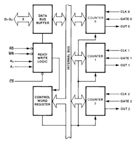
8254 Architecture/ Basic Block Diagram
The architecture/ basic block diagram of 8254 looks as follows −
8254 Pin Description
Here is the pin diagram of 8254 −
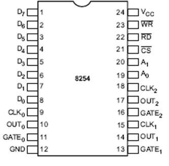
Pin Diagram 8254
In the above figure, there are three counters, a data bus buffer, Read/Write control logic, and a control register. Each counter has two input signals - CLOCK & GATE, and one output signal - OUT.
Data Bus Buffer
It is a tri-state, bi-directional, 8-bit buffer, which is used to interface the 8253/54 to the system data bus. It has three basic functions −
- Programming the modes of 8253/54.
- Loading the count registers.
- Reading the count values.
Read/Write Logic
It includes 5 signals, i.e. RD, WR, CS, and the address lines A0 & A1. In the peripheral I/O mode, the RD and WR signals are connected to IOR and IOW, respectively. In the memory-mapped I/O mode, these are connected to MEMR and MEMW.
Address lines A0 & A1 of the CPU are connected to lines A0 and A1 of the 8253/54, and CS is tied to a decoded address. The control word register and counters are selected according to the signals on lines A0 & A1.
Depending upon the value of CS, A1, and A0 we can determine the addresses of the selected counter.
|
CS |
A1 |
A0 |
SELECTION |
|
0 |
0 |
0 |
C0 |
|
0 |
0 |
1 |
C1 |
|
0 |
1 |
0 |
C2 |
|
0 |
1 |
1 |
Control Register |
This register is accessed when lines A0 & A1 are at logic 1. It is used to write a command word, which specifies the counter to be used, its mode, and either a read or write operation. Following table shows the result for various control inputs.
A1 | A0 | RD | WR | CS | Result |
0 | 0 | 1 | 0 | 0 | Write Counter 0 |
0 | 1 | 1 | 0 | 0 | Write Counter 1 |
1 | 0 | 1 | 0 | 0 | Write Counter 2 |
1 | 1 | 1 | 0 | 0 | Write Control Word |
0 | 0 | 0 | 1 | 0 | Read Counter 0 |
0 | 1 | 0 | 1 | 0 | Read Counter 1 |
1 | 0 | 0 | 1 | 0 | Read Counter 2 |
1 | 1 | 0 | 1 | 0 | No operation |
X | X | 1 | 1 | 0 | No operation |
X | X | X | X | 1 | No operation |
Difference between 8253 and 8254
The following table differentiates the features of 8253 and 8254 −
8253
8254
Its operating frequency is 0 - 2.6 MHz
Its operating frequency is 0 - 10 MHz
It uses N-MOS technology
It uses H-MOS technology
Read-Back command is not available
Read-Back command is available
Reads and writes of the same counter cannot
be interleaved.
Reads and writes of the same counter can be
interleaved.
|
8253 |
8254 |
|
Its operating frequency is 0 - 2.6 MHz |
Its operating frequency is 0 - 10 MHz |
|
It uses N-MOS technology |
It uses H-MOS technology |
|
Read-Back command is not available |
Read-Back command is available |
|
Reads and writes of the same counter cannot
be interleaved. |
Reads and writes of the same counter can be
interleaved. |
Features of 8253 / 54
The
most prominent features of 8253/54 are as follows −
- It has three independent 16-bit down counters.
- It can handle inputs from DC to 10 MHz.
- These three counters can be programmed for either binary or BCD count.
- It is compatible with almost all microprocessors.
- 8254 has a powerful command called READ BACK command, which allows the user to check the count value, the programmed mode, the current mode, and the current status of the counter.
Applications –
- To generate an accurate time delay
- As an event counter
- Square wave generator
- Rate generator
- Digital one shot

Comments
Post a Comment