Programmable Serial Communication Interface 8251 USART
Programmable Serial Communication Interface 8251 USART
8251 universal synchronous asynchronous receiver transmitter (USART) acts as a mediator between the microprocessor and peripheral to transmit serial data into parallel form and vice versa.
- It takes data serially from peripheral (outside devices) and converts it into parallel data.
- After converting the data into parallel form, it transmits it to the CPU.
- Similarly, it receives parallel data from the microprocessor and converts it into serial form.
- After converting data into a serial form, it transmits it to the outside device (peripheral).
The pin description of the 8251A chip

Pin
Description
D0 - D7
parallel data
C/D
Control register or Data buffer select
RD
Read Control
WR
Write control
CS
Chip Select
CLK
clock pulse
RESET
Reset
TxC
Transmitter Clock
TxD
transmitted data
RxC
Receiver Clock
RxD
Receiver Data
RxRDY
Receiver Ready
TxRDY
Transmitter Ready
DSR
Data Set Ready
DTR
Data Terminal Ready
SYNDET/
Synchronous Detect/
BRKDET
DetectBreak
RTS
Request to send Data
CTS
Clear to send Data
TxEMPTY
Transmitter Empty
Vcc
Vcc (5V)
GND
Ground(0V)
The 8251 chip is Universal Synchronous Asynchronous Receiver Transmitter (USART). It acts as a mediator between the microprocessor and peripheral devices. It converts serial data to parallel form and vice versa. This chip is a 28-pin DIP.
There are five different sections in this diagram. These sections are as follows −
- Read/ Write control logic
- Transmitter
- Receiver
- Data Bus Buffer
- Modem Control.
Now let us see the functional block diagram of the 8251 chip.
Block Diagram of 8251 USART –

It contains the following blocks:
1.
Data bus buffer –
This block helps in interfacing the internal data bus of 8251 to the system
data bus. The data transmission is possible between 8251 and CPU by the data
bus buffer block.
2.
Read/Write control logic –
It is a control block for overall device. It controls the overall working by
selecting the operation to be done. The operation selection depends upon input
signals as:

In this way, this unit selects one of the three registers- data buffer register, control register, status register.
- Modem control (modulator/demodulator) –
A device converts analog signals to digital signals and vice-versa and helps the computers to communicate over telephone lines or cable wires. The following are active-low pins of Modem.- DSR: Data Set Ready signal is an input signal.
- DTR: Data terminal Ready is an output signal.
- CTS: It is an input signal which controls the data transmit circuit.
RTS: It is an output signal which is used to set the status RTS.
- Transmit buffer –
This block is used for parallel to serial converter that receives a parallel byte for conversion into serial signal and further transmission onto the common channel.- TXD: It is an output signal, if its value is one, means transmitter will transmit the data.
- Transmit control –
This block is used to control the data transmission with the help of following pins:- TXRDY: It means transmitter is ready to transmit data character.
- TXEMPTY: An output signal which indicates that TXEMPTY pin has transmitted all the data characters and transmitter is empty now.
- TXC: An active-low input pin which controls the data transmission rate of transmitted data.
- Receive buffer –
This block acts as a buffer for the received data.- RXD: An input signal which receives the data.
- Receive control –
This block controls the receiving data. - RXRDY: An input signal indicates that it is ready to receive the data.
- RXC: An active-low input signal which controls the data transmission rate of received data.
- SYNDET/BD: An input or output terminal. External synchronous mode-input terminal and asynchronous mode-output terminal.
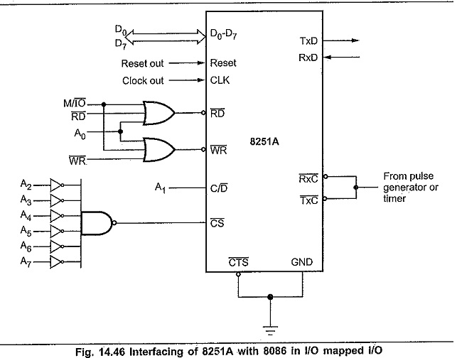
Interfacing 8251A to 8086 in I/O Mapped I/O Mode:
Fig. 14.46 shows the interfacing of 8251A with 8086 in I/O mapped I/O technique. Here, RD and WR signals are activated when M/IO signal is low, indicating I/O bus cycle. Only lower data bus (D0 – D7) is used as 8251A is 8-bit device. Reset out signal from clock generator is connected to the reset signal of the 8251A.
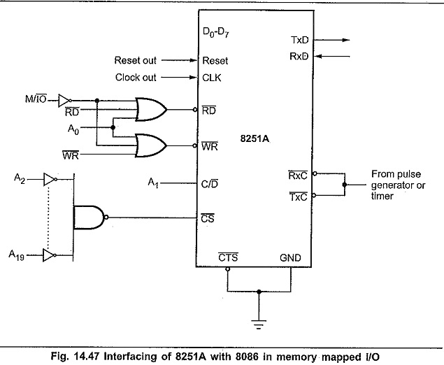
Interfacing 8251A to 8086 in Memory Mapped I/O:
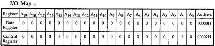
In this type of I/O interfacing, the 8086 uses 20 address lines to identify an I/O device; an I/O device is connected as if it is a memory register. The 8086 uses same control signals and instructions to access I/O as those of memory. Fig. 14.47 shows the interfacing of 8251A with 8086 in memory mapped I/O technique. Here, RD and WR signals are activated when M/IO signal is high, indicating memory bus cycle. Address line A1 is used to select either data register, or control register. The remaining address lines A2-A19 are used to decoder the addresses for 8251A.
Interfacing 8251 with8085
Now let us see how 8251 can be interfaced with 8085. In the diagram, we can see that eight data lines D7-0 are connected to the data bus of the microprocessor. And also the RD and WR of the 8251 are also connected with the RD and RD of 8051. The 8251 is getting the clock from the CLK OUT pin of 8085. And the RESET is also connected to the RESET OUT pin of the microprocessor.
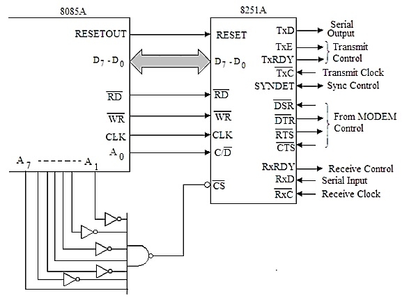
The C/D pin is used to select either control register or data register. This pin is connected to the A0 pin of 8085. The CS pin of 8251 is attached to the output of an address decoder circuit. The address decoder uses A7 to A1 lines of the microprocessor. In this diagram the CS will be enabled when A7 and A4 is at logic 1, and all other lines are at logic 0.
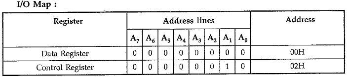
From the following table, we can see how to read or write data word, read the status word and write control word.
Notes :-A0 RD WR Task Port Address 0 0 1 Read Data Word 90H 0 1 0 Write Data Word 90H 1 0 1 Read Status Word 91H 1 1 0 Write Control Word 91H


Comments
Post a Comment