8086 pins configuration
8086 pins configuration
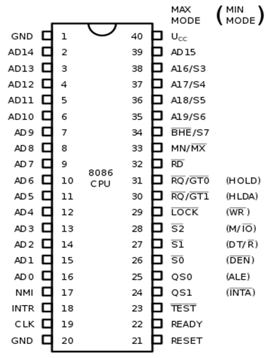
The description of the pins of 8086 is as follows:
AD0-AD15 (Address Data Bus): Bidirectional address/data lines. These are low order address bus. They are multiplexed with data.
When these lines are used to transmit memory address, the symbol A is used instead of AD, for example, A0- A15.
A16 - A19 (Output): High order address lines. These are multiplexed with status signals.
A16/S3, A17/S4: A16 and A17 are multiplexed with segment identifier signals S3 and S4.
A18/S5: A18 is multiplexed with interrupt status S5.
A19/S6: A19 is multiplexed with status signal S6.
BHE/S7 (Output): Bus High Enable/Status. During T1, it is low. It enables the data onto the most significant half of data bus, D8-D15. 8-bit device connected to upper half of the data bus use BHE signal. It is multiplexed with status signal S7. S7 signal is available during T3 and T4.
RD (Read): For read operation. It is an output signal. It is active when LOW.
Ready (Input): The addressed memory or I/O sends acknowledgment through this pin. When HIGH, it denotes that the peripheral is ready to transfer data.
RESET (Input): System reset. The signal is active HIGH.
CLK (input): Clock 5, 8 or 10 MHz.
INTR: Interrupt Request.
NMI (Input): Non-maskable interrupt request.
TEST (Input): Wait for test control. When LOW the microprocessor continues execution otherwise waits.
VCC: Power supply +5V dc.
GND: Ground.
Operating Modes of 8086
There are two operating modes of operation for Intel 8086, namely the minimum mode and the maximum mode.
When only one 8086 CPU is to be used in a microprocessor system, the 8086 is used in the Minimum mode of operation.
In a multiprocessor system 8086 operates in the Maximum mode.
Pin Description for Minimum Mode
In this minimum mode of operation, the pin MN/MX is connected to 5V D.C. supply i.e. MN/MX = VCC.
The description about the pins from 24 to 31 for the minimum mode is as follows:
INTA (Output): Pin number 24 interrupts acknowledgement. On receiving interrupt signal, the processor issues an interrupt acknowledgment signal. It is active LOW.
ALE (Output): Pin no. 25. Address latch enable. It goes HIGH during T1. The microprocessor 8086 sends this signal to latch the address into the Intel 8282/8283 latch.
DEN (Output): Pin no. 26. Data Enable. When Intel 8287/8286 octal bus transceiver is used this signal. It is active LOW.
DT/R (output): Pin No. 27 data Transmit/Receives. When Intel 8287/8286 octal bus transceiver is used this signal controls the direction of data flow through the transceiver. When it is HIGH, data is sent out. When it is LOW, data is received.
M/IO (Output): Pin no. 28, Memory or I/O access. When this signal is HIGH, the CPU wants to access memory. When this signal is LOW, the CPU wants to access I/O device.
WR (Output): Pin no. 29, Write. When this signal is LOW, the CPU performs memory or I/O write operation.
HLDA (Output): Pin no. 30, Hold Acknowledgment. It is sent by the processor when it receives HOLD signal. It is active HIGH signal. When HOLD is removed HLDA goes LOW.
HOLD (Input): Pin no. 31, Hold. When another device in microcomputer system wants to use the address and data bus, it sends HOLD request to CPU through this pin. It is an active HIGH signal.
Pin Description for Maximum Mode
In the maximum mode of operation, the pin MN/¯MX is made LOW. It is grounded. The description about the pins from 24 to 31 is as follows:
QS1, QS0 (Output): Pin numbers 24, 25, Instruction Queue Status. Logics are given below:
| QS1 | QS0 | Operation |
|---|---|---|
| 0 | 0 | No operation |
| 0 | 1 | 1st byte of opcode from queue. |
| 1 | 0 | Empty the queue |
| 1 | 1 | Subsequent byte from queue |
S0, S1, S2 (Output): Pin numbers 26, 27, 28 Status Signals. These signals are connected to the bus controller of Intel 8288. This bus controller generates memory and I/O access control signals. Logics for status signal are given below:
| S2 | S1 | S0 | Operation |
|---|---|---|---|
| 0 | 0 | 0 | Interrupt acknowledgement |
| 0 | 0 | 1 | Read data from I/O port |
| 0 | 1 | 0 | Write data from I/O port |
| 0 | 1 | 1 | Halt |
| 1 | 0 | 0 | Opcode fetch |
| 1 | 0 | 1 | Memory read |
| 1 | 1 | 0 | Memory write |
| 1 | 1 | 1 | Passive state |
LOCK (Output): Pin no. 29. It is an active LOW signal. When this signal is LOW, all interrupts are masked and no HOLD request is granted. In a multiprocessor system all other processors are informed through this signal that they should not ask the CPU for relinquishing the bus control.
RG/GT1, RQ/GT0 (Bidirectional): Pin numbers 30, 31, Local Bus Priority Control. Other processors ask the CPU by these lines to release the local bus.
In the maximum mode of operation signals WR, ALE, DEN, DT/R etc. are not available directly from the processor. These signals are available from the controller 8288.


Comments
Post a Comment