Architecture of 8086
A Microprocessor is an Integrated Circuit with all the functions of a CPU. However, it cannot be used stand-alone since unlike a microcontroller it has no memory or peripherals.
8086 does not have RAM or ROM inside it. However, it has internal registers for storing intermediate and final results and interfaces with memory located outside it through the System Bus.
In the case of 8086, it is a 16-bit Integer processor in a 40-pin, Dual Inline Packaged IC.
The size of the internal registers(present within the chip) indicates how much information the processor can operate on at a time (in this case 16-bit registers) and how it moves data around internally within the chip, sometimes also referred to as the internal data bus.
8086 provides the programmer with 14 internal registers, each of 16 bits or 2 bytes wide. The main advantage of the 8086 microprocessor is that it supports Pipelining.


8086 Architecture
Memory segmentation:
- In order to increase execution speed and fetching speed, 8086 segments the memory.
- Its 20-bit address bus can address 1MB of memory, it segments it into 16 64kB segments.
- 8086 works only with four 64KB segments within the whole 1MB memory.
The internal architecture of Intel 8086 is divided into 2 units: The Bus Interface Unit (BIU), and The Execution Unit (EU). These are explained as following below.
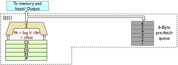
1. The Bus Interface Unit (BIU):
It provides the interface of 8086 to external memory and I/O devices via the System Bus. It performs various machine cycles such as memory read, I/O read, etc. to transfer data between memory and I/O devices.
BIU performs the following functions are as follows:
- It generates the 20-bit physical address for memory access.
- It fetches instructions from the memory.
- It transfers data to and from the memory and I/O.
- Maintains the 6-byte pre-fetch instruction queue(supports pipelining).
BIU mainly contains the 4 Segment registers, the Instruction Pointer, a pre-fetch queue, and an Address Generation Circuit.
Instruction Pointer (IP):
- It is a 16-bit register. It holds offset of the next instructions in the Code Segment.
- IP is incremented after every instruction byte is fetched.
- IP gets a new value whenever a branch instruction occurs.
- CS is multiplied by 10H to give the 20-bit physical address of the Code Segment.
- The address of the next instruction is calculated by using the formula CS x 10H + IP.
Example:
CS = 4321H IP = 1000H
then CS x 10H = 43210H + offset =  44210H
Here Offset = Instruction Pointer(IP)
This is the address of the next instruction.
Code Segment register: (16 Bit register): CS holds the base address for the Code Segment. All programs are stored in the Code Segment and accessed via the IP.
Data Segment register: (16 Bit register): DS holds the base address for the Data Segment.
Stack Segment register: (16 Bit register): SS holds the base address for the Stack Segment.
Extra Segment register: (16 Bit register): ES holds the base address for the Extra Segment.
Please note that segments are present in memory and segment registers are present in Microprocessor.
Segment registers store starting address of each segments in memory.
Address Generation Circuit:
- The BIU has a Physical Address Generation Circuit.
- It generates the 20-bit physical address using Segment and Offset addresses using the formula:
- In Bus Interface Unit (BIU) the circuit shown by the Σ symbol is responsible for the calculation unit which is used to calculate the physical address of an instruction in memory.
Physical Address = Segment Address x 10H + Offset Address6 Byte Pre-fetch Queue:
- It is a 6-byte queue (FIFO).
- Fetching the next instruction (by BIU from CS) while executing the current instruction is called pipelining.
- Gets flushed whenever a branch instruction occurs.
- The pre-Fetch queue is of 6-Bytes only because the maximum size of instruction that can have in 8086 is 6 bytes. Hence to cover up all operands and data fields of maximum size instruction in 8086 Microprocessor there is a Pre-Fetch queue is 6 Bytes.
- The pre-Fetch queue is connected with the control unit which is responsible for decoding op-code and operands and telling the execution unit what to do with the help of timing and control signals.
- The pre-Fetch queue is responsible for pipelining and because of that 8086 microprocessor is called the fetch, decode, execute type microprocessor. Since there are always instructions present for decoding and execution in this queue the speed of execution in the microprocessor is gradually increased.
- When there is a 2-byte space in the instruction pre-fetch queue then only the next instruction will be pushed into the queue otherwise if only a 1-byte space is vacant then there will not be any allocation in the queue. It will wait for spacing of 2 bytes in subsequent queue decoding operations.
- Instruction pre-fetch queue works in a sequential manner so if there is any branch condition then in that situation pre-fetch queue fails. Hence to avoid chaos instruction queue is flushed out when any branch or conditional jumps occur.
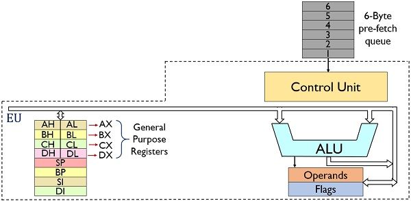
2. The Execution Unit (EU):
The main components of the EU are General purpose registers, the ALU, Special purpose registers, the Instruction Register and Instruction Decoder, and the Flag/Status Register.
- Fetches instructions from the Queue in BIU, decodes, and executes arithmetic and logic operations using the ALU.
- Sends control signals for internal data transfer operations within the microprocessor.(Control Unit)
- Sends request signals to the BIU to access the external module.
- It operates with respect to T-states (clock cycles) and not machine cycles.
8086 has four 16-bit general purpose registers AX, BX, CX, and DX which store intermediate values during execution. Each of these has two 8-bit parts (higher and lower).
- AX register: (Combination of AL and AH Registers)
It holds operands and results during multiplication and division operations. Also an accumulator during String operations.
- BX register: (Combination of BL and BH Registers)
It holds the memory address (offset address) in indirect addressing modes.
- CX register: (Combination of CL and CH Registers)
It holds the count for instructions like a loop, rotates, shifts and string operations.
- DX register: (Combination of DL and DH Registers)
It is used with AX to hold 32-bit values during multiplication and division.
Arithmetic Logic Unit (16-bit): Performs 8 and 16-bit arithmetic and logic operations.
Special purpose registers (16-bit): Special purpose registers are called Offset registers also. Which points to specific memory locations under each segment.
We can understand the concept of segments as Textbook pages. Suppose there are 10 chapters in one textbook and each chapter takes exactly 100 pages. So the book will contain 1000 pages. Now suppose we want to access page number 575 from the book than 500 will be the segment base address which can be anything in the context of microprocessors like Code, Data, Stack, and Extra Segment. So 500 will be segment registers that are present in Bus Interface Unit (BIU). And 500 + 75 is called an offset register through which we can reach on specific page number under a specific segment.
Hence 500 is the segment base address and 75 is an offset address or (Instruction Pointer, Stack Pointer, Base Pointer, Source Index, Destination Index) any of the above according to their segment implementation.
- Stack Pointer: Points to Stack top. Stack is in Stack Segment, used during instructions like PUSH, POP, CALL, RET etc.
- Base Pointer: BP can hold the offset addresses of any location in the stack segment. It is used to access random locations of the stack.
- Source Index: It holds offset address in Data Segment during string operations.
- Destination Index: It holds offset address in Extra Segment during string operations.
Instruction Register and Instruction Decoder:
The EU fetches an opcode from the queue into the instruction register. The instruction decoder decodes it and sends the information to the control circuit for execution.
Flag/Status register (16 bits): It has 9 flags that help change or recognize the state of the microprocessor.
6 Status flags:
- Carry flag(CF)
- Parity flag(PF)
- Auxiliary carry flag(AF)
- Zero flags (Z)
- Sign flag(S)
- Overflow flag (O)
Status flags are updated after every arithmetic and logic operation.
3 Control flags:
- Trap flag(TF)
- Interrupt flag(IF)
- Direction flag(DF)
These flags can be set or reset using control instructions like CLC, STC, CLD, STD, CLI, STI, etc. The Control flags are used to control certain operations.
Execution of whole 8086 Architecture:
- All instructions are stored in memory hence to fetch any instruction first task is to obtain the Physical address of the instruction is to be fetched. Hence this task is done by Bus Interface Unit (BIU) and by Segment Registers. Suppose the Code segment has a Segment address and the Instruction pointer has some offset address then the physical address calculator circuit calculates the physical address in which our instruction is to be fetched.
- After the address calculation instruction is fetched from memory and it passes through C-Bus (Databus) as shown in the figure, and according to the size of the instruction, the instruction pre-fetch queue fills up. For example MOV AX, BX is 1 Byte instruction so it will take only the 1st block of the queue, and MOV BX,4050H is 3 Byte instruction so it will take 3 blocks of the pre-fetch queue.
- When our instruction is ready for execution, according to the FIFO property of the queue instruction comes into the control system or control circuit which resides in the Execution unit. Here instruction decoding takes place. The decoding control system generates an opcode that tells the microprocessor unit which operation is to be performed. So the control system sends signals all over the microprocessor about what to perform and what to extract from General and Special Purpose Registers.
- Hence after decoding microprocessor fetches data from GPR and according to instructions like ADD, SUB, MUL, and DIV data residing in GPRs are fetched and put as ALU’s input. and after that addition, multiplication, division, or subtraction whichever calculation is to be carried out.
- According to arithmetic, flag register values change dynamically.
- While Instruction was decoding and executing from step 3 of our algorithm, the Bus interface Unit doesn’t remain idle. it continuously fetches an instruction from memory and put it in a pre-fetch queue and gets ready for execution in a FIFO manner whenever the time arrives.
- So in this way, unlike the 8085 microprocessor, here the fetch, decode, and execution process happens in parallel and not sequentially. This is called pipelining, and because of the instruction pre-fetch queue, all fetching, decoding, and execution process happen side-by-side. Hence there is partitioning in 8086 architecture like Bus Interface Unit and Execution Unit to support Pipelining phenomena.
Working of 8086 Microprocessor
In the previous section, we have discussed the operation of various sections of the BIU and EU. Now in this section, we will have a look at the overall processing cycle of the 8086 microprocessors. So, basically, when an instruction is to be fetched from the memory, then firstly its physical address must be calculated and this is done at the BIU. The physical address of an instruction is given as:
PA = Segment address Χ 10 + Offset
For example: Suppose the segment address is 2000 H and the offset address is 4356 H. So, the generated physical address is 24356 H. Here, the code segment register provides the base address of the code segment which is combined with the offset address.
The code segment contains the instructions. Each time an instruction is fetched the offset address inside the code segment gets incremented. So, once the physical address of an instruction is calculated by the BIU of the processor, it sends the memory location by the address bus to the memory. Further, the desired instruction at that memory location which is present in the form of the opcode is fetched by the microprocessor through the data bus.
Suppose the instruction is ADD BL, CL. But, inside the memory, it will be in the form of an opcode. So, this opcode is sent to the control unit.
The control unit decodes the opcode and generates control signals that inform the BL and CL register to release the value stored in it. Also, it signals the ALU to perform the ADD operation on that particular data.
It is noteworthy that in any instruction, like ADD BL, CL. BL denotes the destination of the result of the add operation. This clearly shows that whatever, the operation is performed its result must be stored in the first register i.e., BL for this particular example.
Let us take another example: Consider an instruction, ADD CL, 05H.
This means that the operand which is 05H is to be added with the data present in the CL register and is stored in that particular register i.e., CL. In such conditions, the operand is not provided to the control unit as only the opcode is required to be decoded by the CU. Hence the operand is directly provided to the ALU. Also, the status of this result is stored in the flag register. So, whenever, ALU carries out an operation, it simultaneously generates the result as well as its status.
It is to be noteworthy that in BIU, pipelining fails whenever there is branching in the instruction. This is because generally instructions are present in a sequential manner. But, sometimes the instructions are required to be executed unsequentially. However, in the queue, the instructions are stored sequentially. So, in case there exist a need for any random instruction to be decoded. The opcode stored in the queue will become invalid and must be cleared at that particular time.
So, this is all about the block diagram and working of the 8086 microprocessor.
Comments
Post a Comment