Minimum mode configuration of 8086 microprocessor (Min mode)
Overview :
The 8086 microprocessor operates in minimum mode when MN/MX’ = 1.
In minimum mode,8086 is the only processor in the system which provides all the control signals which are needed for memory operations and I/O interfacing.
Here the circuit is simple but it does not support multiprocessing.
The other components which are transceivers, latches, 8284 clock generator, 74138 decoder, memory and i/o devices are also present in the system.
The address bus of 8086 is 20 bits long. By this we can access 220 byte memory i.e. 1MB . Out of 20 bits, 16 bits A0 to A15(or 16 lines) are multiplexed with a data bus. By multiplexing, it means they will act as address lines during the first T state of the machine cycle and in the rest, they act as data lines. A16 to A19 are multiplexed S3 to S6 and BHE’ is multiplexed with S7.
Maximum mode of 8086 block diagram
Control signals provided by 8086 for memory operations and i/o interfacing : They are used to identifying whether the bus is carrying a valid address or not , in which direction data is needed to be transferred over the bus, when there is valid write data on the data bus and when to put read data on the system bus. Therefore, their sequence pattern makes all the operations successful in a particular machine cycle.
Min mode circuit
Minimum Mode Circuit
8282:
It is an 8-bit latch.
Basically it is a buffered D flip flop.
This latch separates the multiplexed address received from the data bus by using control signal ALE. This ALE signal is an active high signal.
This ALE signal is connected to the strobe of the latch.
We need 3 latches here because the address is 20 bits.
8286:
8286 is an 8-bit transceiver.
They are data amplifiers and act as bidirectional buffers.
This trans receivers separates the multiplexed address received from the address or data bus.
Since the data bus is 16 bits we require 2 trans receivers.
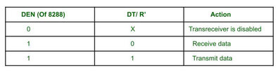
This transceiver is connected to signals DT/R’ and DEN’. These signals are enabled using DEN signals.
DT/R’ controls the direction of data on the control bus and it is also connected to T and DEN’.
8284:
It is a clock generator used to provide clocks.
There is Input/ output transfer from the bus when signal M/IO’= 1. Also, when the signal M/IO’ = 0 input/output operations are performed.
The read (RD’) and write (WR’) signals are used to differentiate whether a read bus cycle or write bus cycle is performing.
When signal WR’=0 it performs write operation and when RD’=0 the microprocessor 8086 performs read operation.
The signal DEN is also used with RD’. This signal enables the external devices so that they can put data on the bus.
All these control signals (M/IO’, RD’, WR’) are decoded using a 3:8 decoder. Ic 74138 is a 3:8 decoder.
INTR and INTA :
These are interrupt signals of an 8086 microprocessor. Whenever there is an interrupt from external devices to 8086 INTR=1.
When the processor is ready to provide service to external devices then signal INTA’= 0.
The other devices can make bus requests by sending signal HOLD.
The 8086 acknowledges them through HLDA signals in return.
Timing diagram of 8086 Minimum Mode:
Opcode fetch / Read Timing Diagram
The processor cannot get the control of the bus until the master does not set HLDA=0.
Write Memory Cycle
The timing diagram of 8086 minimum mode operation is explained below.
There are four t-states of the bus cycle for microprocessor 8086.
These T-states are T1,T2,T3 and T4
During the T1 state the processor gives the address on the bus for 1 T-state.
In T2 state the processor changes the bus direction.
In T3 and T4 states the data is transferred.
The wait signal is also generated betweenT3 and T4 states.
8282 (8 bits) latch : The latches are buffered D FF. They are used to separate the valid address from the multiplexed Address/data bus by using the control signal ALE, which is connected to strobe(STB) of 8282. The ALE is active high signal. Here three such latches are required because the address is 20 bits.
8286 (8 bits) transceivers : They are bidirectional buffers and also known as data amplifiers. They are used to separate the valid data from multiplexed add/data bus. Two such transceivers are needed because the data bus is 16 bits long. 8286 is connected to DT/R’ and DEN’ signals. They are enabled through the DEN signal .The direction of data on the data bus is controlled by the DT/R’ signal. DT/R’ is connected to T and DEN’ is connected to OE’.
Direction of data flow
8284 clock generator is used to provide the clock.
M/IO’= 1,then I/O transfer is performed over the bus. and when M/IO’ = 0, then I/O operation is performed.
The signals RD’ and write WR’ are used to identify whether a read bus cycle or a write bus cycle is performing. When WR’ = 0 ,then it indicates that valid output data on the data bus.
RD’ indicates that the 8086 is performing a read data or instruction fetch process is occurring .During read operations, one other control signal is also used, which is DEN ( data enable) and it indicates the external devices when they should put data on the bus.
Control signals for all operations are generated by decoding M/IO’, RD’, WR’. They are decoded by 74138 3:8 decoder.
INTR and INTA : When INTR = 1,then there is an interrupt to 8086 by other devices for their service. When INTA’= 0,then it indicates that the processor is ready to service them.
The bus request is made by other devices using the HOLD signal and the processor acknowledges them using the HLDA output signal.
For more details about the 8086 minimum mode pins please refer(this article).
Timing diagram : The working of min mode can be easily understood by timing diagrams.
All processors bus cycle is of at least 4 T-states(T1,T2,T3,T4) .The address is given by processor in the T1 state. It is available on the bus for one T-state.
In T2, the bus is tristated for changing the direction of the bus( in the case of a data read cycle.)
The data transfer takes place between T3 and T4.
If the addressed device is slower, then the wait state is inserted between T3 and T4.
Opcode fetch or read timing diagram
At T1 state ALE =1 ,this indicates that a valid address is latched on the address bus and also M / IO’= 1, which indicates the memory operation is in progress.
In T2, the address is removed from the local bus and is sent to the addressed device. Then the bus is tristated.
When RD’ = 0 , the valid data is present on the data bus.
During T2 DEN’ =0, which enables transceivers and DT/R’ = 0 ,which indicates that the data is received.
During T3, data is put on the data bus and the processor reads it.
The output device makes the READY line high. This means the output device has performed the data transfer process. When the processor makes the read signal to 1, then the output device will again tristate its bus drivers.
Write memory cycle
At T1 state ALE =1 ,this indicates that a valid address is latched on the address bus and also M / IO’= 1, which indicates the memory operation is in progress.
In T2, the processor sends the data to be written to the addressed location.
The data is buffered on the bus until the middle of T4 state.
The WR’=0 becomes at the beginning of T2.
The BHE’ and A0 signals are used to select the byte or bytes of memory or I/O word.
During T2 DEN’ =0, which enables, transceivers and DT/R’ = 1 ,which indicates that the data is transferred by the processor to the addressed device.
All kinds of memory and i/o operations are performed using the decoding of M/IO’and RD’ WR’ as shown in the table above.
Maximum mode configuration of 8086 microprocessor (Max mode)
8086 microprocessor characteristics:
It contains 20 bit address bus.
It contains 16-bit data bus, therefore 8086 is called as 16-bit microprocessor.
It is 2-stage pipelined processor. It can prefetch 6 bytes from memory and store into queue to increase the speed of the execution.
It’s control bus carries signals for executing operations such as read ,write etc.
It has Memory Banks. 2 banks of 512KB each. These banks are called as lower Bank (even) and higher Bank (odd).
In 8086 the entire memory is divided into four memory segments which are code ,stack, data and extra segment.
8086 has 16 bit IO address.
It has 256 interrupts.
8086 has two operating Modes:
Minimum mode
Maximum mode
Minimum mode:
In this 8086 is the only processor in the system. In a minimum mode 8086 system.
8086 is operated in minimum mode when MN/MX’ pin to logic 1.
In this mode, all the control signals are given out by the 8086 itself.
Maximum mode:
In this we can connect more processors to 8086 (8087/8089).
8086 max mode is basically for implementation of allocation of global resources and passing bus control to other coprocessor (i.e. second processor in the system), because two processors can not access system bus at same instant.
All processors execute their own program.
The resources which are common to all processors are known as global resources.
The resources which are allocated to a particular processor are known as local or private resources.
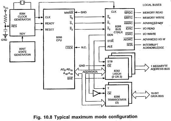
Maximum mode circuit
Circuit explanation:
When MN/ MX’ = 0 , 8086 works in max mode.
Clock is provided by 8284 clock generator.
8288 bus controller- Address form the address bus is latched into 8282 8-bit latch. Three such latches are required because address bus is 20 bit. The ALE(Address latch enable) is connected to STB(Strobe) of the latch. The ALE for latch is given by 8288 bus controller.
The data bus is operated through 8286 8-bit transceiver. Two such transceivers are required, because data bus is 16-bit. The transceivers are enabled the DEN signal, while the direction of data is controlled by the DT/R signal. DEN is connected to OE’ and DT/ R’is connected to T. Both DEN and DT/ R’ are given by8288 bus controller.
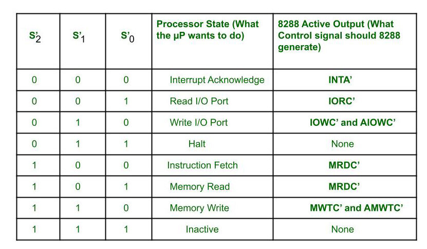
Control signals for all operations are generated by decoding S’2, S’1 and S’0 using 8288 bus controller.
Bus request is done using RQ’ / GT’ lines interfaced with 8086. RQ0/GT0 has more priority than RQ1/GT1.
INTA’ is given by 8288, in response to an interrupt on INTR line of 8086.
In max mode, the advanced write signals get enabled one T-state in advance as compared to normal write signals. This gives slower devices more time to get ready to accept the data, therefore it reduces the number of cycles.
Advantages of max mode of 8086:
It helps to interface more devices like 8087.This interface is also called a closely coupled co-Processor configuration. In this 8086 is called as the host and 8087 as Co-processor.
It supports multiprocessing, Therefore it helps to increase efficiency.
The 8087 was the first floating-point coprocessor for the 8086 series of microprocessors. The purpose of the 8087 was to increase calculations for floating point operations, such as add, sub, multiply, divide, and square root.
Disadvantages of max mode over min mode :
It has more complex circuit than min mode.
Applications of 8086:
Microcomputer are built using 8086. For example: IBM PC, used the Intel 8088, a version of the 8086 with 8-bit data bus.
It is used in calculators.
It is used for control purposes like in traffic signals(uses microcontrollers which are nothing but contains one or more CPUs along with memory and programmable i/o peripherals).
Minimum mode
Maximum mode
In minimum mode there can be only one processor i.e. 8086.
In maximum mode there can be multiple processors with 8086, like 8087 and 8089.
MN/MX¯¯¯¯¯¯¯¯¯¯is 1 to indicate minimum mode.
MN/MX¯¯¯¯¯¯¯¯¯¯is 0 to indicate maximum mode.
ALE for the latch is given by 8086 as it is the only processor in the circuit.
ALE for the latch is given by 8288 bus controller as there can be multiple processors in the circuit.
DEN¯¯¯¯¯¯¯¯¯¯¯¯and DT/R¯¯¯¯for the trans-receivers are given by 8086 itself.
and DT/R¯¯¯¯ for the trans-receivers are given by 8288 bus controller.
Direct control signals M/IO¯¯¯¯¯¯, RD¯¯¯¯¯¯¯¯ and WR¯¯¯¯¯¯¯¯¯are given by 8086.
Instead of control signals, each processor generates status signals called S2¯¯¯¯¯, S1¯¯¯¯¯ and S0¯¯¯¯¯.
Control signals M/IO¯¯¯¯¯¯, RD¯¯¯¯¯¯¯¯and WR¯¯¯¯¯¯¯¯¯are decoded by a 3:8 decoder like 74138.
Status signals S2¯¯¯¯¯, S1¯¯¯¯¯ and S0¯¯¯¯¯are decoded by a bus controller like 8288 to produce control signals.
INTA¯¯¯¯¯¯¯¯¯¯¯¯¯¯ is given by 8086 in response to an interrupt on INTR line.
INTA¯¯¯¯¯¯¯¯¯¯¯¯¯¯is given by 8288 bus controller in response to an interrupt on INTR line.
HOLD and HLDA signals are used for bus request with a DMA controller like 8237.
RQ¯¯¯¯¯¯¯¯/GT¯¯¯¯¯¯¯¯,lines are used for bus requests by other processors like 8087 or 8089.
The circuit is simpler.
The circuit is more complex.
Multiprocessing cannot be performed hence performance is lower.
As multiprocessing can be performed, it can give very high performance.
Microprocessor and Microcontroller Assignment Questions Instructions: · Solve any 8 questions in each section. · Make appropriate assumptions wherever necessary. Unit 1 1. What is microprocessor? 2. What is the difference between the microprocessor and microcontroller? 3. Explain the register organization of 8086 4. How many data lines and address lines are available in 8086? 5. Explain briefly about the internal hardware architecture of 8086 microprocessor with a neat diagram 6. What is the maximum memory size that can be addressed by 8086? 7. Calculate the physical address for fetching the next instruction to be executed, in 8086? 8. ...
A Microprocessor is an Integrated Circuit with all the functions of a CPU. However, it cannot be used stand-alone since unlike a microcontroller it has no memory or peripherals . 8086 does not have RAM or ROM inside it. However, it has internal registers for storing intermediate and final results and interfaces with memory located outside it through the System Bus. In the case of 8086, it is a 16-bit Integer processor in a 40-pin, Dual Inline Packaged IC. The size of the internal registers(present within the chip) indicates how much information the processor can operate on at a time ( in this case 16-bit registers ) and how it moves data around internally within the chip, sometimes also referred to as the internal data bus. 8086 provides the programmer with 14 internal registers, each of 16 bits or 2 bytes wide. The main advantage of the 8086 microprocessor is that it supports Pipelining. 8086 Architecture M...
8254 is a device designed to solve the timing control problems in a microprocessor. It has 3 independent counters, each capable of handling clock inputs up to 10 MHz, and size of each counter is 16 bit. It operates in +5V regulated power supply and has 24 pin signals. All modes are software programmable. The 8254 is an advanced version of 8253 which did not offered the feature of read back command. 8254 Architecture/ B asic Block Diagram The architecture/ basic block diagram of 8254 looks as follows − 8254 Pin Description Here is the pin diagram of 8254 − Pin Diagram 8254 In the above figure, there are three counters, a data bus buffer, Read/Write control logic, and a control register. Each counter has two input signals - CLOCK & GATE, and one output signal - OUT. Data Bus Buffer It is a tri-state, bi-directional, 8-bit buffer, which is used to interface the 8253/54 to the system data bus. It has three basic functions − Programming the modes of 8253/54. Loading t...


Comments
Post a Comment